Company Advantages1. Strictly complying with the CCC standard, ADV
impedance pcb is manufactured with higher quality in terms of security and reliability. For example, its internal and external wires are designed with a high security guarantee.
2. The substrate of this product features improved heat dissipation, greatly lowering the operating temperature. Thus, it counts a lot in extending its service life.
3. To assure its quality, the product is manufactured under the supervision of our experienced QA team.
4. By setting up the quality assurance system, ADV has enough capability to produce exquisite
via in pad pcb with high quality.
5. There has been a rapid development of Shenzhen ADV Technology Co., Ltd. in terms of economic strength, market management and product R&D strength.
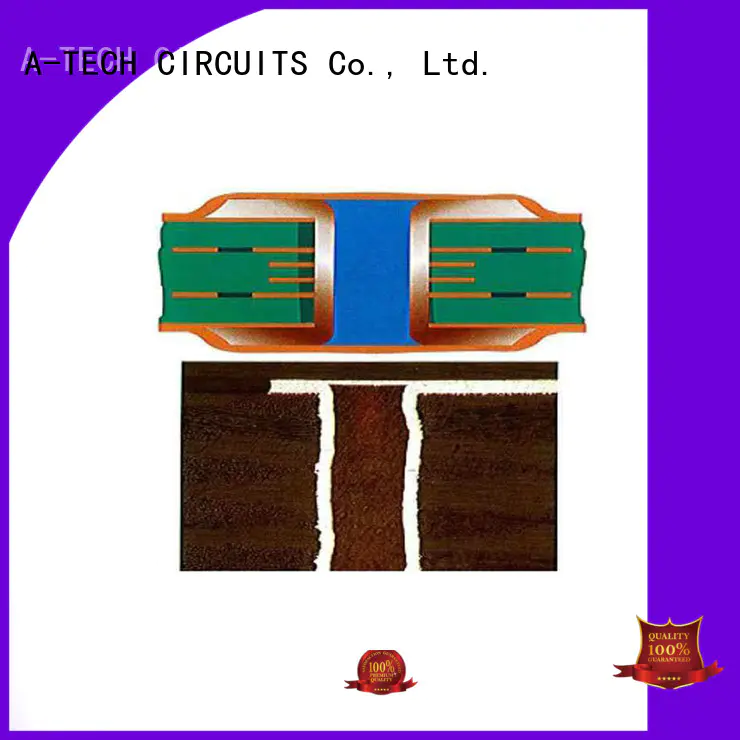
Via In Pad (VIP) technology refers to the vias in SMD pad or BGA pad due to small space for layout, in order to avoid the solder paste flow into inner layer or the other side in assembly production, basically this type of via need to be plugged with resin and plate copper over to cap the via to make it invisible.
Via in pad technology is widely used in high density PCBs, especially for the PCBs that require a limited BGA space and are focused on heat transfer and high speed design. Although blind holes and buried holes help increasing density and save space on the circuit boards, through holes are still the best choice for thermal management and high speed design elements.
The advantages of Via In Pad technology
● Suitable for fine pitch BGAs
● Improved thermal dissipation
● Provides a flat, coplanar surface for component attachment
● Leading to higher density of PCBs and promoting space saving
● Overcomes high speed design issues and constraints.
● Meets closely packed placement requirements.
The Via In Pad technology is defined in IPC standard with IPC-4761 VII
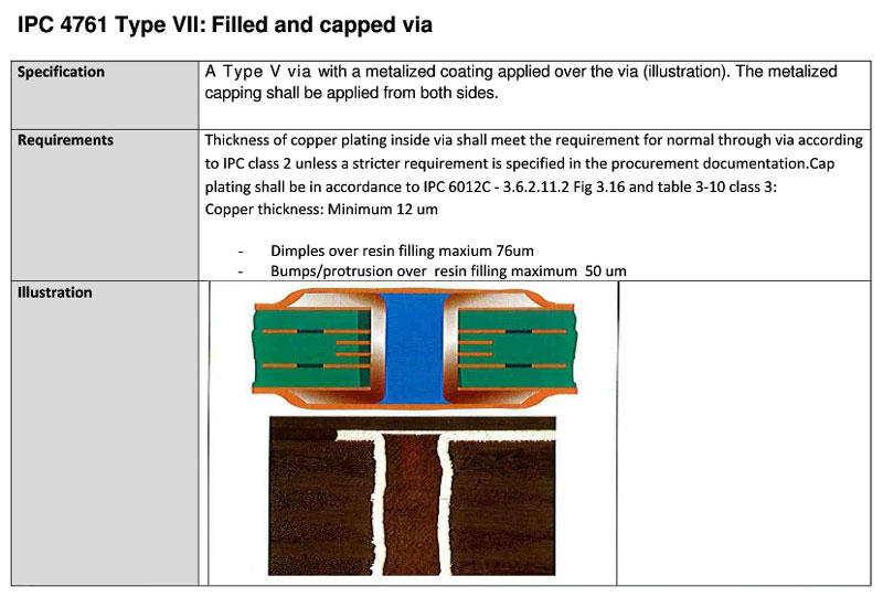
ADV manufactured lots of multilayer PCBs with Via In Pad designs Both in BGA Pads or in other SMD Pads, we’re able to plugged vias fully and then plated copper over to make the surface of pad as flat as other pads without dimples.
Company Features1. Shenzhen ADV Technology Co., Ltd. is a specialist in the creation of via in pad pcb , all along the value chain from product development to manufacturing.
2. Our quality is our company name card in
hybrid pcb industry, so we will do it best.
3. Shenzhen ADV Technology Co., Ltd. will consistently execute the business theory of impedance pcb . Get price! Promoting heavy copper pcb to achieve the value of ADV is the goal of the company. Get price! The core concept of Shenzhen ADV Technology Co., Ltd. is to create thoughtful products for everyday living. Get price! ADV aims to provide the best shopping experience to not only create value for consumers but company. Get price!


 pусский


