Company Advantages1. The manufacturinhg process of ADV enig pcb has been optimized to ensure that key parameters can be achieved, such as function, physical space, standby, maintenance, capital, and operating costs, environmental impacts, and more.
2. The quality of this product has met the requirements of international standards.
3. To ensure the high quality, the product has been strictly tested under the quality control standards.
4. With good quality,
carbon ink pcb and stylish design, our products are extensively used in many industries.
5. Quality for enig pcb is always put in very important place in Shenzhen ADV Technology Co., Ltd..
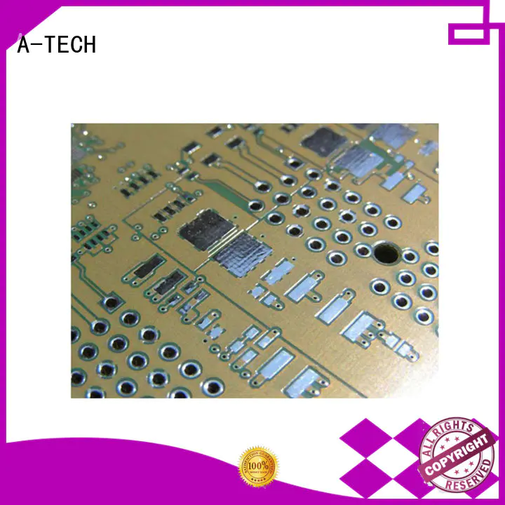
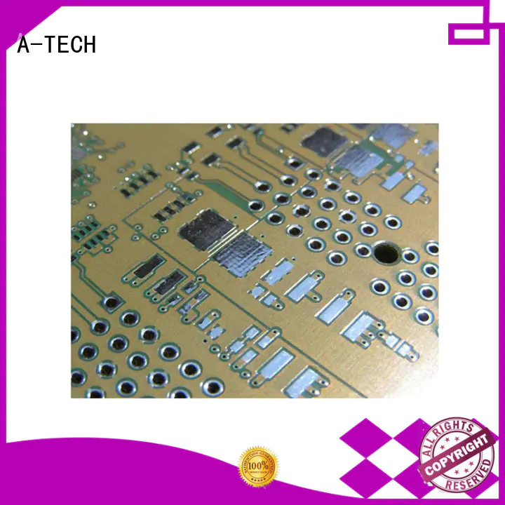
HAL(Lead Free), the full name is Hot Air leveling with Lead Free. Compared with HASL, the main difference for HAL(Lead Free) is the element of material which do not contain Lead(Pb), so it’s RoHS Compliant and it’s much more popular and widely used in PCB manufacturing.
HAL(Lead Free) requires higher run temperatures for lead free solder and longer contact time, the production cost for HAL(Lead Free) is slightly higher than HASL(Tin/Lead).
The manufacturing process of HAL(Lead Free) is similar to HASL(Tin/Lead), the circuit boards will be submersed in molten solder(Lead Free). This solder will cover all the exposed copper surfaces. Upon retraction from the solder, high pressure hot air is blown over the surface through air knives, this levels the solder deposit and removes the excess solder from the surface of printed circuit boards.
The typical thickness of HAL(Lead Free) is 1-40um and the shelf life is 12 months.
The advantages of HAL(Lead Free) surface finish
● Good solderability / wettability
● RoHS Compliant
● Good reflow properties
● Large processing window is allowed
● Multiple thermal excursions
● Can be widely used
The disadvantages of HAL(Lead Free) surface finish
● Uneven surface
● Not suitable for PCBs with fine pitch
● Thermal shock
● Solder bridge
● Plugged or Reduced plated through holes
ADV have HAL(Lead Free) surface finish in house, It’s basically the highest proportion of finish used for circuit boards without fine pitch or high density layout. We don’t have any additional cost for HAL(Lead Free) surface finish.
Company Features1. Shenzhen ADV Technology Co., Ltd. is a enig pcb manufacturer dedicated to design, development, production and sales.
2. Our factory is supported by a series of manufacturing facilities. They allow us to offer full-scale production and meet a wide variety of customer and market needs while maintaining the highest possible quality.
3. For several decades, Shenzhen ADV Technology Co., Ltd. has constantly adopted the ceremony tenet of commitment and honesty. Check it! ADV will invest a lot of money in production peelable mask pcb . Check it! Shenzhen ADV Technology Co., Ltd. is dedicated to becoming a comprehensive osp pcb supplier with international influence. Check it! Shenzhen ADV Technology Co., Ltd. hopes to guide the development of the pcb surface finish market. Check it!


 pусский


