Company Advantages1. The design of ADV
countersink pcb is good. It is inspired by many sources, such as fashion market research which offers detail information about the latest trends, most usable color, consumer demands, and preferable fabric.
2. The product is highly resistant to bacteria. Thanks to the nature of the materials used and the sealant on top, it will not be able to absorb any bacteria.
3. Shenzhen ADV Technology Co., Ltd. always provides maximum support to customers to achieve win-win collaboration.
4. Shenzhen ADV Technology Co., Ltd. has good communication and marketing ability.
PCB with Blind and Buried Vias
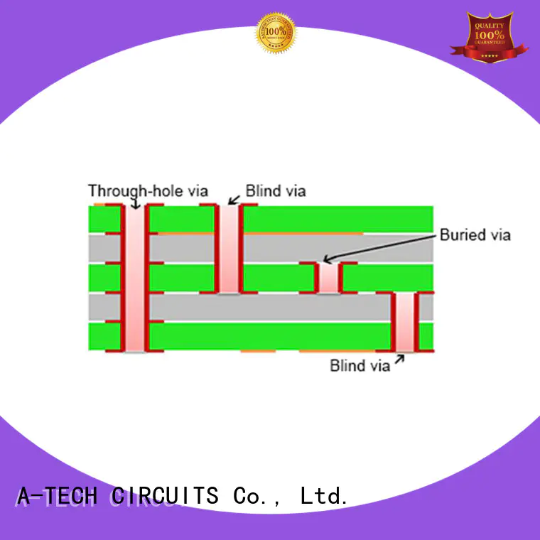
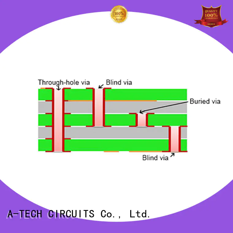
Basically the blind and buried vias are popular to be designed on high density PCBs due to the limit of small space, the blind and buried vias can only pass through necessary layers and more surface area become available for components, they have the ability to meet the density constraints of line and pads on a typical design without increasing the layer count or board size and reduce the PCB aspect ratio for convenient production.
Blind Vias
Blind via is a copper plated hole that connects only one outer layer to one or more inner layers, it never goes all the way through a circuit board but only visible on one side of circuit boards. The blind via can be laser or mechanically drilled based on the detailed via hole size and layer stackup.
Buried Vias
Buried Via is a copper plated hole that connects two or more inner layers without contacting the outer layers, as the name suggests, it’s buried inside, so it’s not visible from the outer layer of PCB. Buried via has no impact to any trace or surface mount component on the top or bottom layers, trace or SMD pad can be placed directly over the buried via.
ADV CIRCUITS has capacity to build both of blind via and buried via with different demands, We’ll use laser drill for the blind vias with size smaller than 150um and use mechanical drill for the blind via size larger than 150um, the technology of blind via we can achieve include via in pad, stacked via and staggered via. The minimum size of buried via normally need to be 150um and they’ll be plugged with resin to avoid prepreg flow into buried via which might affect the connection with adjacent layers.
Company Features1. As a mature and advanced company, ADV always provides customers with the best countersink pcb .
2. Shenzhen ADV Technology Co., Ltd. has established strong talent advantages in
blind vias pcb development.
3. ADV will be committed to providing customers with via in pad pcb and services with ultimate experience. Get more info! Shenzhen ADV Technology Co., Ltd. emphasizes the importance of honest and friendly relationship with our customers. Get more info! It is very urgent for ADV to adapt to the rapid development of globalization and information technology. Get more info! Our operating philosophy states that Shenzhen ADV Technology Co., Ltd. is our customer's 'first partner'. Get more info!


 pусский


