-
 pусский

pусский
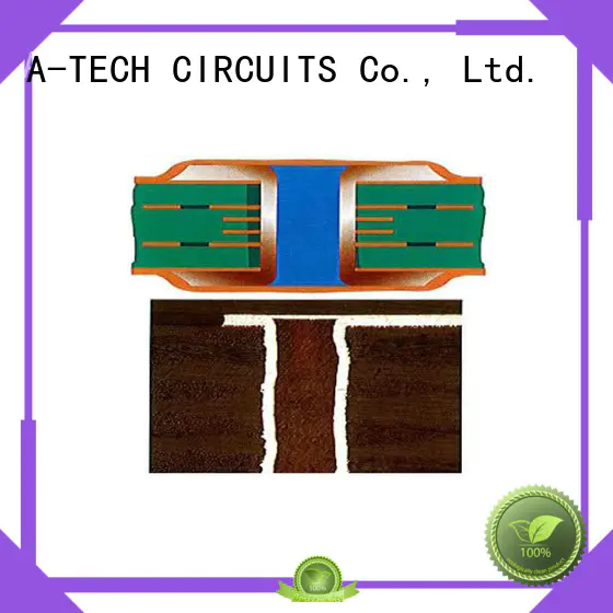


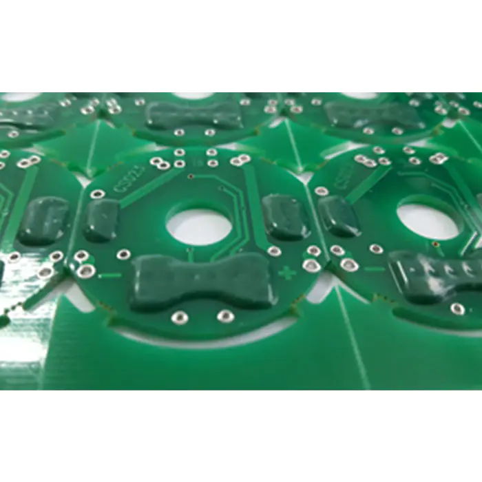
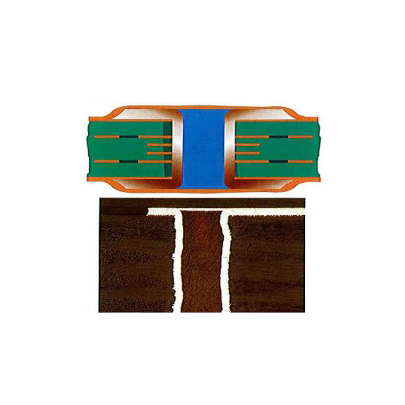
Via In Pad (VIP) technology refers to the vias in SMD pad or BGA pad due to small space for layout, in order to avoid the solder paste flow into inner layer or the other side in assembly production, basically this type of via need to be plugged with resin and plate copper over to cap the via to make it invisible.
Via in pad technology is widely used in high density PCBs, especially for the PCBs that require a limited BGA space and are focused on heat transfer and high speed design. Although blind holes and buried holes help increasing density and save space on the circuit boards, through holes are still the best choice for thermal management and high speed design elements.
The advantages of Via In Pad technology
● Suitable for fine pitch BGAs
● Improved thermal dissipation
● Provides a flat, coplanar surface for component attachment
● Leading to higher density of PCBs and promoting space saving
● Overcomes high speed design issues and constraints.
● Meets closely packed placement requirements.
The Via In Pad technology is defined in IPC standard with IPC-4761 VII
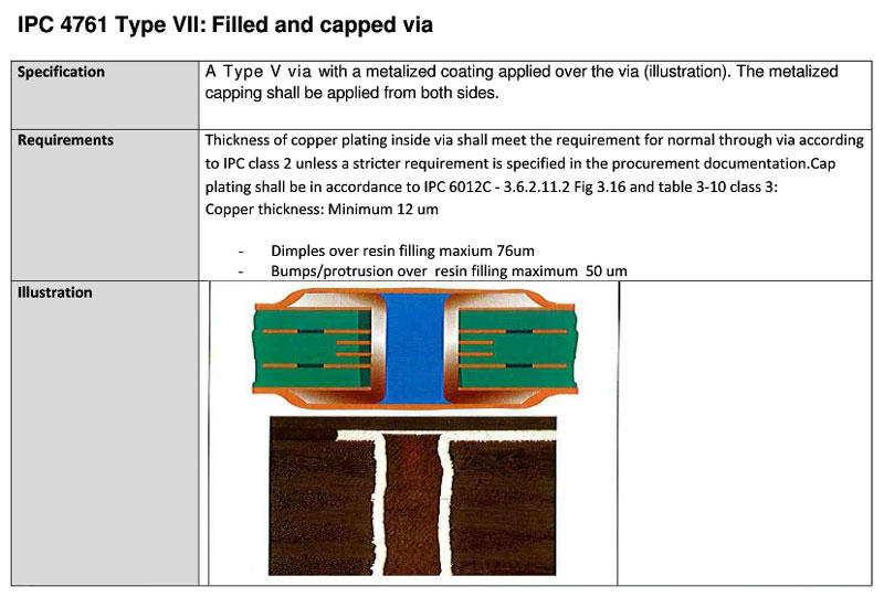
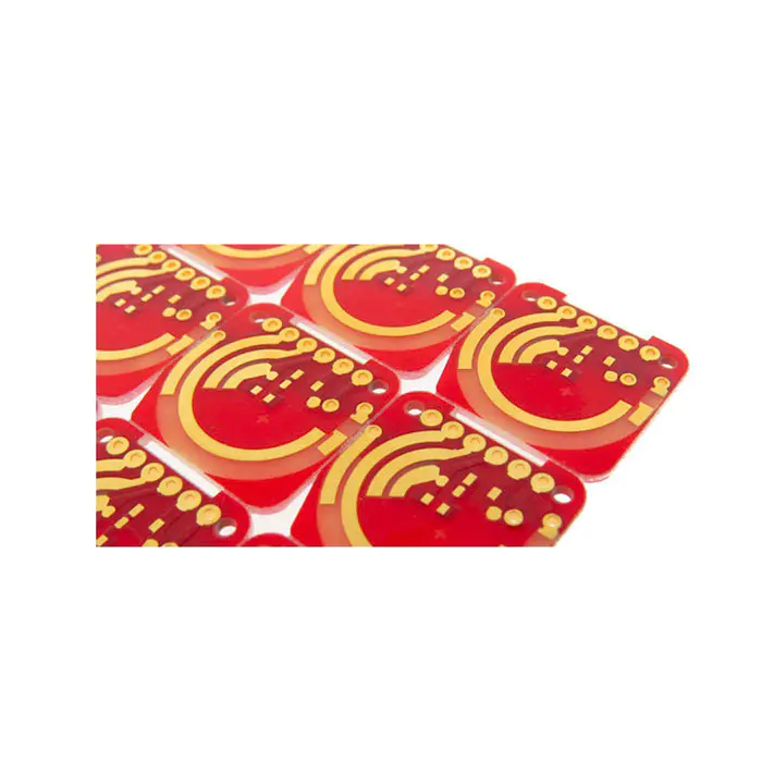
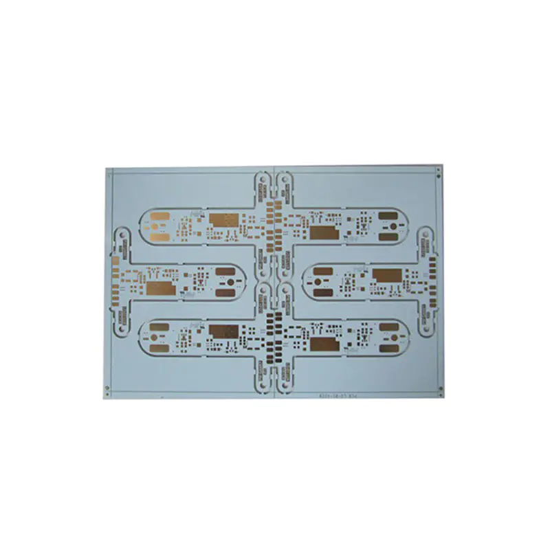
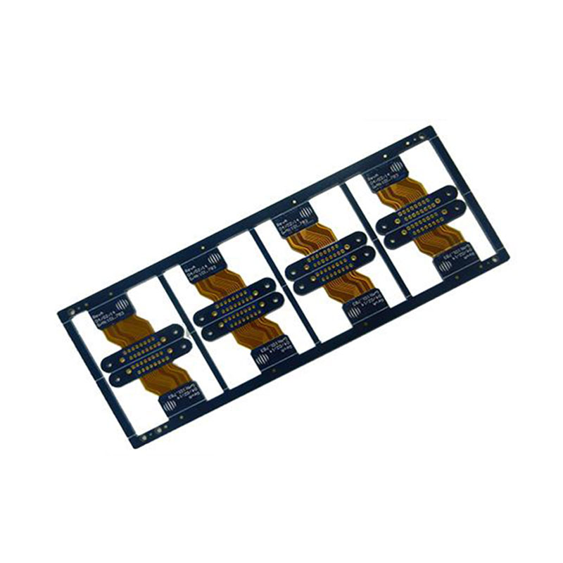
ADV manufactured lots of multilayer PCBs with Via In Pad designs Both in BGA Pads or in other SMD Pads, we’re able to plugged vias fully and then plated copper over to make the surface of pad as flat as other pads without dimples.
General inquiries & Customer Service
Tel: 86-755-2335 9479 | Fax: 86-755-3318 0911
E-Mail: JacekKutkowska757@gmail.com
Skype: advchcircuits
QUICK LINKS
→ HOME
→ ABOUT US
→ PCB MANUFACTURING
→ PCB ASSEMBLY
→ CAPABILITY
→ RESOURCES
→ CONTACT US
PCB MANUFACTURING

Headquarters: No.9 Datong Road, Shenzhen, Guangdong China
Copyright ? 2025 Shenzhen ADV Technology Co., Ltd. | All Rights Reserved
Hello, please leave your name and email here before chat online so that we won't miss your message and contact you smoothly.