Company Advantages1. ADV press fit pins pcb is strictly measured. It is measured using highly sophisticated and computerized machines in term of distance, angle, diameter, and radius. It has low water absorptivity in the damp environment
2. Breakthrough progress has been made in ADV with its high quality
thick copper pcb . The product is certified under UL(E357001) and RoHS
3. This product has perfect quality and our team has a rigorous attitude of continuous improvement on this product. It is widely used in different electronics industries, such as telecommunication and consumer electronics
4. The product is quality assured as it has passed the ISO certification. It totally conforms to the UL Flame Rating of 94V-0
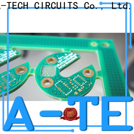
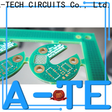
Depth control routing(milling) is also known as Z-axis milling or level milling, it refers to partial routing in printed circuit board manufacturing with a variable level elevation at the PCB edge or within PCB.
Control depth routing technology supports a high end market with the need for accuracy, miniaturization, process stability and the need for productivity, and depth routing option allows for very complex designs, bended boards and structures to be processed with fine precision.
Depth control routing technology have great advantages in PCB assembly as the special shape of depth routing.
● It can avoid cold soldering as siphonic effect use NPTH step stair slot
● Use the step stair in middle of PCB apply in special module application, and degrade the height of PCB assembly, achieve refinement and miniaturization
● Use the step stair of PCB edge make card slot is favor for PCB fixed and installation
● Use Special size NPTH step stair as resonant cavity of microwave signal, degrade signal loss and other special function.
ADV has manufacturing capability to build various types of depth routing with different size and depth, no matter on the PCB edge or within the PCB, and the precision tolerance can be controlled as +/-0.1mm(4mil).
Company Features1. Shenzhen ADV Technology Co., Ltd. is a Chinese company. Our meticulous attention to press fit pins pcb design and manufacturing makes us trustworthy. Shenzhen ADV Technology Co., Ltd. assembles many professional elites in thick copper pcb field.
2. With strong technical expertise and advanced management, Shenzhen ADV Technology Co., Ltd. produces many kinds of
blind vias pcb .
3. Shenzhen ADV Technology Co., Ltd. has equipped the global advanced machines. Shenzhen ADV Technology Co., Ltd. will shoulder corporate social responsibility, and dedicated to innovative, harmonious and green development. Ask!


 pусский